
Piezoelectric-on-Insulator (POI) Wafer MarketSize, Share & Industry Analysis, 2026-2034By Piezoelectric MaterialBy Substrate TypeBy Wafer SizeBy ApplicationBy Bonding and Thinning MethodBy Piezoelectric Layer ThicknessBy Filter Technology ServedBy Operating Frequency BandBy Supplier TypeBy Customer TypeBy Sales Channel
Full title & scope — all 11 axes with their segments
Piezoelectric-on-Insulator (POI) Wafer Market Size, Share & Industry Analysis, By Piezoelectric Material (Lithium Tantalate, Lithium Niobate, Other Piezoelectric Films), By Substrate Type (Silicon, Silicon Oxide, Sapphire, Other Substrates), By Wafer Size (100 mm, 150 mm, 200 mm, 300 mm), By Application (TF-SAW Filters for 4G/5G/6G Handsets, IoT and Wireless Connectivity, Automotive, Infrastructure, Other RF), By Bonding and Thinning Method (Fusion / Direct Bonding, Smart Cut-type Layer Transfer, Grinding and Polishing), By Piezoelectric Layer Thickness (Below 0.5 µm, 0.5 – 1 µm, 1 – 5 µm, Above 5 µm), By Filter Technology Served (Temperature-compensated SAW, Thin-film SAW, Bulk Acoustic Wave (BAW) Alternatives, Conventional SAW), By Operating Frequency Band (Below 1 GHz, 1 – 3 GHz, 3 – 6 GHz, Above 6 GHz), By Supplier Type (Engineered Substrate Makers, Piezoelectric Crystal Producers, Silicon Wafer Manufacturers, Filter IDMs with In-house Bonding, Foundry and Bonding Service Providers), By Customer Type (Integrated Device Manufacturers, Fabless Filter Companies, RF Foundries, Research Institutes and Pilot Lines), By Sales Channel (Direct Long-term Supply Agreements, Spot and Sample Sales, Distributors, Toll Processing / Co-development), and Regional Forecast, 2026-2034
Market outlook, key takeaways, drivers and challenges for the report period.
- 01By Piezoelectric MaterialLithium Tantalate · Lithium Niobate · Other Piezoelectric Films
- 02By Substrate TypeSilicon · Silicon Oxide · Sapphire
- 03By Wafer Size100 mm · 150 mm · 200 mm
- 04By ApplicationTF-SAW Filters for 4G/5G/6G Handsets · IoT and Wireless Connectivity · Automotive
- 05By Bonding and Thinning MethodFusion / Direct Bonding · Smart Cut-type Layer Transfer · Grinding and Polishing
- 06By Piezoelectric Layer ThicknessBelow 0.5 µm · 0.5 – 1 µm · 1 – 5 µm
- 07By Filter Technology ServedTemperature-compensated SAW · Thin-film SAW · Bulk Acoustic Wave
- 08By Operating Frequency BandBelow 1 GHz · 1 – 3 GHz · 3 – 6 GHz
- 09By Supplier TypeEngineered Substrate Makers · Piezoelectric Crystal Producers · Silicon Wafer Manufacturers
- 10By Customer TypeIntegrated Device Manufacturers · Fabless Filter Companies · RF Foundries
- 11By Sales ChannelDirect Long-term Supply Agreements · Spot and Sample Sales · Distributors
- 12By Region
Market Analysis & Outlook
Piezoelectric-on-insulator wafers are engineered substrates in which a thin film of single-crystal lithium tantalate, lithium niobate or another piezoelectric material is bonded to a carrier such as silicon, silicon oxide on silicon or sapphire. The film is thinned to a controlled thickness so that surface acoustic wave filters built on it hold their frequency across temperature and reach a higher quality factor than filters cut from bulk crystal. Buyers are filter makers and RF foundries that fabricate filters for handsets, connectivity modules, vehicles and base stations, along with research institutes running pilot lines.
The global piezoelectric-on-insulator (poi) wafer market stood at USD 420 million in 2025. A forecast-period rate of 15% takes it to USD 1545 million by 2034, and the study reports every year in between, passing USD 150 million in 2020, USD 345 million in 2024, USD 505 million in 2026 and USD 945 million in 2030.
On the piezoelectric material axis, growth rates run from 13.88% for Lithium Tantalate (LT) up to 16.73% for Lithium Niobate (LN). Lithium Tantalate (LT) carries the volume: USD 252 million and 60% of revenue in 2025, USD 849.75 million and 55% in 2034. Lithium Niobate (LN) take share over the period; Lithium Tantalate (LT) and Other Piezoelectric Films give it up while still growing in absolute terms.
The substrate type split puts Silicon first, at USD 260.4 million and 62% of revenue in 2025, rising to USD 865.2 million and 56% in 2034. Silicon Oxide (SiO2-on-Si) grows faster at 18.77% against 14.27%, moving from 18% of revenue to 23% by 2034. It cuts the same total as the piezoelectric material axis from a different commercial angle, so revenue does not add across the two.
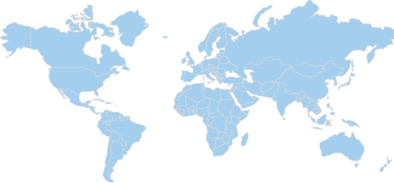
Geographically, 65% of 2025 revenue sits in Asia Pacific (USD 273 million rising to USD 1035.15 million) ahead of Europe at 19% and USD 79.8 million. Middle East and Africa is smallest, at 1%. Share shifts toward Asia Pacific over the forecast period, so the regional split repays a close reading.
Behind these figures sit five regions, three piezoelectric material lines and eleven segmentation axes, each reported for every year from 2020 to 2034. The headline 2025 value is arrived at by triangulating published aggregates against category proxies, not by an independent count, and the same applies to the segment, regional and country breakdowns drawn from it.
Market Size, 2020–2034
USD MillionRevenue in USD Million. Values up to 2025 are actuals; 2026–2034 are forecast.
Key Takeaways
- A forecast-period rate of 15% takes the market from USD 420 million in 2025 to USD 1545 million in 2034, against 22.87% recorded over the 2020-2025 historical period.
- 60% of 2025 revenue sits in Lithium Tantalate (LT) (USD 252 million) and it remains the largest piezoelectric material line in 2034 at USD 849.75 million and 55%.
- At 16.73%, Lithium Niobate (LN) grows faster than any other piezoelectric material line, moving from USD 147 million and 35% of revenue in 2025 to USD 618 million and 40% in 2034.
- Against a base case of USD 1545 million in 2034, the study also reports a bear case at USD 1266.9 million and a bull case at USD 1823.1 million, with the assumptions behind each set out separately.
- 65% of 2025 revenue is generated in Asia Pacific, worth USD 273 million and rising to USD 1035.15 million by 2034; Middle East and Africa is smallest at 1%.
- 35.9% of Asia Pacific's base-year revenue comes from Japan alone: USD 98 million in 2025, rising to USD 330 million by 2034, which is why it is that region's worked example.
- Every line on all eleven segmentation axes and in each of the five regions carries its own revenue, share and growth rate for all fifteen years, 2020 through 2034, on a 2025 base.
Market Trends
Revenue Share, By piezoelectric material
Base year 2025Lithium Tantalate (LT) leads with 60.0% of piezoelectric material segment revenue.
Share of piezoelectric material segment revenue, most recent base year.
Read across the forecast period, the global piezoelectric-on-insulator (poi) wafer market shows movement in three places: piezoelectric material composition, regional weight, and the 15% rate applied to the whole.
The direction of the market is not in question in any of the three. Each line and each region grows in revenue terms; what separates them is which takes the larger part of the growth.
Lithium Niobate (LN) grows faster than Lithium Tantalate (LT). Lithium Niobate (LN) grows at 16.73% across 2026-2034 against 13.88% for Lithium Tantalate (LT), the widest spread on the piezoelectric material axis. Lithium Niobate (LN) takes its share of revenue from 35% to 40% while Lithium Tantalate (LT) gives up ground, from 60% to 55%. Neither contracts: USD 147 million becomes USD 618 million, USD 252 million becomes USD 849.75 million. What the spread decides is which of them a supplier's revenue is exposed to.
Regional weight shifts toward Asia Pacific. Asia Pacific moves from 65% of revenue in 2025 to 67% in 2034, worth USD 273 million rising to USD 1035.15 million. Against that, North America at 14% moving to 14%, Europe at 19% moving to 17%, Latin America at 1% moving to 1%, Middle East and Africa at 1% moving to 1%, a fall in share, not in revenue. Revenue added in this market is therefore concentrating geographically instead of spreading evenly, and a participant weighted toward a share-losing region grows more slowly than the market even while its own revenue climbs.
Growth compounds at 15% without a step change. Year by year the total runs USD 150 million in 2020, USD 345 million in 2024, USD 420 million in 2025, USD 505 million in 2026, USD 945 million in 2030 and USD 1545 million in 2034. Against 22.87% through the historical period, the 15% forecast rate is a continuation; no year in the series interrupts it. The risk in the number sits in the mix assumptions, not in whether the market grows at all, which is where the piezoelectric material and regional sections come in.
Market Growth Factors
Growth is concentrated in Lithium Niobate (LN)
Market Drivers
3- 01Growth is concentrated in Lithium Niobate (LN)
Lithium Niobate (LN) compounds at 16.73% against 15% for the market, rising from USD 147 million in 2025 to USD 618 million in 2034 and from 35% of revenue to 40%. Nothing else on the axis grows as fast (Lithium Tantalate (LT) manages 13.88%) so the blended 15% is carried by this one line instead of shared across them. That makes position on the piezoelectric material axis a growth decision, not a product one.
- 02Growth lands where the revenue already is
65% of 2025 revenue (USD 273 million) is generated in Asia Pacific, reaching USD 1035.15 million by 2034, with share rising to 67%. Behind it, Europe holds 19%; USD 79.8 million rising to USD 262.65 million. Because both the existing revenue and the revenue added concentrate in these two, regional weighting matters more to a forecast than regional count does.
- 03Fifteen years of unbroken growth underpin the forecast
Revenue rose through USD 150 million in 2020, USD 345 million in 2024 and USD 420 million in 2025, a compound 22.87% across the historical period. From there the forecast carries 15% through to USD 1545 million in 2034. Fifteen years of unbroken growth in the series means the forecast rests on a demonstrated trajectory, not a projected turnaround, and it is why the 15% rate is applied flat across the whole period instead of ramped through it.
Growth drivers
| # | Growth driver | Impact | Gross contribution (USD Million) | 2026-28 | 2029-31 | 2032-34 |
|---|---|---|---|---|---|---|
| 1 | Migration of handset filters to thin-film SAW on POI wafers | High | +520 | High | High | Medium |
| 2 | Rising RF filter content per handset from added 5G and 6G bands | High | +330 | High | Medium | Medium |
| 3 | Transition to 200 mm and 300 mm wafers lowering cost per die | Medium-High | +180 | Medium | High | High |
| 4 | Adoption in IoT, automotive and infrastructure RF | Medium | +160 | Low | Medium | High |
| 5 | Domestic filter supply chain build-out in Asia | Medium | +90 | Medium | Medium | Low |
| 6 | Others | Low | +45 | Low | Low | Low |
| Total | +1325 | |||||
Restraints
| # | Restraint | Impact | Estimated reduction (USD Million) | 2026-28 | 2029-31 | 2032-34 |
|---|---|---|---|---|---|---|
| 1 | Bonding yield losses and high process cost on thin films | Medium-High | −90 | High | Medium | Medium |
| 2 | Competition from bulk acoustic wave and conventional SAW filters | Medium | −70 | Medium | Medium | High |
| 3 | Crystal supply concentration and export controls | Medium | −40 | Medium | Medium | Low |
| Total | −200 | |||||
Drivers contribute 1325 USD Million and restraints remove 200 USD Million, a net 1125 USD Million, which is the revenue the market adds between the base year and 2034. Contributions are CDI estimates, apportioned so that they reconcile with the forecast rather than being read from it.
The 15% forecast rate rests on three things that can be measured separately: the size of the existing base, the mix shift on the piezoelectric material axis, and where regional growth is concentrated.
Restraining Factors
Downside case: USD 1266.9 million by 2034, against USD 1545 million in the base case
Market Restraints
2- 01Downside case: USD 1266.9 million by 2034, against USD 1545 million in the base case
The study's downside path assumes bulk acoustic wave designs keep the premium bands, bonding yields on larger wafers stall, and crystal export restrictions or weaker handset volumes slow wafer purchases, and ends 2034 at USD 1266.9 million against the USD 1545 million base case, the same USD 420 million base year, a slower forecast period.
- 02Lithium Tantalate (LT) holds the blended rate down
With 60% of 2025 revenue (USD 252 million) Lithium Tantalate (LT) is where most of the market sits, and it grows at only 13.88% against the market's 15%. Revenue still reaches USD 849.75 million by 2034 and share still falls to 55%: a drag on the average, not a decline.
Market Opportunities
Upside case: USD 1823.1 million by 2034
Market Opportunities
2- 01Upside case: USD 1823.1 million by 2034
A bull case of USD 1823.1 million by 2034, against USD 1545 million in the base case, turns on a single stated assumption: thin-film SAW takes most mid-band handset filters earlier than planned, 300 mm bonding yields improve quickly, and 6G bands and automotive qualification add demand before the end of the decade. The USD 420 million 2025 base is common to both.
- 02The opening is on the piezoelectric material axis, not the regional one
Lithium Niobate (LN) grows at 16.73% against 15% for the market, adding revenue from USD 147 million in 2025 to USD 618 million in 2034 and taking its share from 35% to 40%. It is the place on this axis where share changes hands at scale, so it is where an entrant can take position without displacing the incumbent in Lithium Tantalate (LT).
Market Challenges
The total depends on a single line
Market Challenges
2- 01The total depends on a single line
One line dominates: Lithium Tantalate (LT), at 60% of revenue in 2025 and 55% in 2034, worth USD 252 million and USD 849.75 million. No other single change on the piezoelectric material axis moves the total as much as a change in demand for that one line.
- 02Asia Pacific is largely Japan
Japan generates USD 98 million of Asia Pacific's USD 273 million in 2025, 35.9% of the region, reaching USD 330 million by 2034. A regional number that depends this heavily on one country carries that country's specific conditions inside it, which a reader treating the region as diversified would miss.
Segmentation Analysis
11 axeseleven segmentation axes are reported; by piezoelectric material, by substrate type, wafer size, application, bonding and thinning method, piezoelectric layer thickness, filter technology served, operating frequency band, supplier type, customer type and sales channel. Revenue does not add across them: each is a different cut of the same total.
Three piezoelectric material lines are reported. One of them takes share over the forecast period and the rest give it up, though every line grows in absolute terms between 2025 and 2034.
By Piezoelectric Material · 3 segments
Lithium Tantalate (LT) Led by Piezoelectric material in 2025, with Lithium Niobate (LN) Growing Fastest
- Largest Lithium Tantalate (LT) · 60%
- Fastest Lithium Niobate (LN) · 16.7%
- Moves most Lithium Tantalate (LT) · -5 pts
- Order by 2034 unchanged
| Segment | 2025 | Share | 2034 | Share | CAGR |
|---|---|---|---|---|---|
| Lithium Tantalate (LT) | $252M | 60% | $850M | 55%-5 | 13.9% |
| Lithium Niobate (LN) | $147M | 35% | $618M | 40%+5 | 16.7% |
| Other Piezoelectric Films | $21M | 5% | $77.25M | 5% | 15% |
Lithium tantalate leads because it became the standard film for thin-film SAW filters in handsets, with well-understood cut angles and a long qualification record. Lithium niobate grows fastest because its stronger coupling suits wider-bandwidth filters in higher bands, and more suppliers now bond it at production scale. Other films remain small and exploratory. By 2034 Lithium Tantalate (LT) is still ahead, making this a shift in weight, not a change of leader. Every year of the series is priced on this axis, making it the reference cut for the rest of the report.
By Substrate Type · 4 segments
Silicon Led by Substrate type in 2025, with Silicon Oxide (SiO2-on-Si) Growing Fastest
- Largest Silicon · 62%
- Fastest Silicon Oxide (SiO2-on-Si) · 18.8%
- Moves most Silicon · -6 pts
- Order by 2034 unchanged
| Segment | 2025 | Share | 2034 | Share | CAGR |
|---|---|---|---|---|---|
| Silicon | $260M | 62% | $865M | 56%-6 | 14.3% |
| Silicon Oxide (SiO2-on-Si) | $75.60M | 18% | $355M | 23%+5 | 18.8% |
| Sapphire | $50.40M | 12% | $185M | 12% | 15.6% |
| Other Substrates | $33.60M | 8% | $139M | 9%+1 | 17.1% |
Silicon leads because it is inexpensive, available in every wafer diameter and compatible with standard fabrication tools, and it adds the temperature stability that filters need. Silicon oxide on silicon grows fastest because the oxide layer improves acoustic confinement and filter performance in higher bands. Sapphire serves niche high-performance uses, and other substrates are early in qualification. By 2034 Silicon is still ahead, making this a shift in weight, not a change of leader.
By Wafer Size · 4 segments
150 mm (6-inch) Led by Wafer size in 2025, with 300 mm (12-inch) Growing Fastest
- Largest 150 mm (6-inch) · 52%
- Fastest 300 mm (12-inch) · 30.6%
- Moves most 150 mm (6-inch) · -14 pts
- Order by 2034 changes
| Segment | 2025 | Share | 2034 | Share | CAGR |
|---|---|---|---|---|---|
| 100 mm (4-inch) | $33.60M | 8% | $46.35M | 3%-5 | 3.6% |
| 150 mm (6-inch) | $218M | 52% | $587M | 38%-14 | 11.6% |
| 200 mm (8-inch) | $151M | 36% | $726M | 47%+11 | 19.1% |
| 300 mm (12-inch) | $16.80M | 4% | $185M | 12%+8 | 30.6% |
The six-inch size leads because most thin-film SAW filter lines were set up around it and early handset volumes were qualified there. The twelve-inch size grows fastest from a small base because larger wafers lower cost per die once bonding yield is proven, and a few lines are moving to it. The four-inch size loses share as legacy lines retire. By 2034 the largest line is 200 mm (8-inch) and no longer 150 mm (6-inch), the one axis here where the order actually changes.
By Application · 5 segments
Automotive Outpaces the Axis While TF-SAW Filters for 4G/5G/6G Handsets Holds the Largest Share
- Largest TF-SAW Filters for 4G/5G/6G Handsets · 78%
- Fastest Automotive · 20.9%
- Moves most TF-SAW Filters for 4G/5G/6G Handsets · -8 pts
- Order by 2034 unchanged
| Segment | 2025 | Share | 2034 | Share | CAGR |
|---|---|---|---|---|---|
| TF-SAW Filters for 4G/5G/6G Handsets | $328M | 78% | $1082M | 70%-8 | 14.2% |
| IoT and Wireless Connectivity | $33.60M | 8% | $170M | 11%+3 | 19.7% |
| Automotive | $25.20M | 6% | $139M | 9%+3 | 20.9% |
| Infrastructure | $21M | 5% | $92.70M | 6%+1 | 17.9% |
| Other RF | $12.60M | 3% | $61.80M | 4%+1 | 19.3% |
Handset filters lead because every 5G phone carries many filters and thin-film SAW suits the mid and high bands where temperature drift matters. Automotive grows fastest as connected vehicles add cellular, satellite and positioning radios that need dependable filters across wide temperature ranges. Infrastructure and connectivity follow, while other RF uses stay small. By 2034 TF-SAW Filters for 4G/5G/6G Handsets is still ahead, making this a shift in weight, not a change of leader.
By Bonding and Thinning Method · 3 segments
Smart Cut-type Layer Transfer Held the Dominant Share of the Bonding and thinning method Segment in 2025
- Largest Smart Cut-type Layer Transfer · 60%
- Fastest Grinding and Polishing (Bond-and-Thin) · 16.4%
- Moves most Fusion / Direct Bonding · -3 pts
- Order by 2034 unchanged
| Segment | 2025 | Share | 2034 | Share | CAGR |
|---|---|---|---|---|---|
| Fusion / Direct Bonding | $105M | 25% | $340M | 22%-3 | 13.9% |
| Smart Cut-type Layer Transfer | $252M | 60% | $958M | 62%+2 | 16% |
| Grinding and Polishing (Bond-and-Thin) | $63M | 15% | $247M | 16%+1 | 16.4% |
Smart Cut-type layer transfer leads because it gives thin, uniform films and reuses donor crystal, which suits high-volume production. Grinding and polishing grows fastest as lower-cost lines in Asia use it to serve thicker film products. Direct bonding as a stand-alone route loses share since most volume now uses layer transfer. By 2034 Smart Cut-type Layer Transfer is still ahead, making this a shift in weight, not a change of leader.
By Piezoelectric Layer Thickness · 4 segments
0.5 – 1 µm Held the Dominant Share of the Piezoelectric layer thickness Segment in 2025
- Largest 0.5 – 1 µm · 50%
- Fastest Below 0.5 µm · 17.9%
- Moves most 0.5 – 1 µm · -6 pts
- Order by 2034 changes
| Segment | 2025 | Share | 2034 | Share | CAGR |
|---|---|---|---|---|---|
| Below 0.5 µm | $84M | 20% | $371M | 24%+4 | 17.9% |
| 0.5 – 1 µm | $210M | 50% | $680M | 44%-6 | 13.9% |
| 1 – 5 µm | $92.40M | 22% | $371M | 24%+2 | 16.7% |
| Above 5 µm | $33.60M | 8% | $124M | 8% | 15.6% |
Mid-thin films lead because they match the wavelengths of the main handset bands. The thinnest films grow fastest as higher-frequency filters demand ever thinner layers, which raises the difficulty of thinning and the price per wafer. Thicker films serve lower-frequency and specialist uses and hold their position. The order does not change: 0.5 – 1 µm is still largest in 2034, and what moves is how much it holds.
By Filter Technology Served · 4 segments
By Filter Technology Served
- Largest Thin-film SAW (TF-SAW / IHP-SAW) · 45%
- Fastest Thin-film SAW (TF-SAW / IHP-SAW) · 19.8%
- Moves most Thin-film SAW (TF-SAW / IHP-SAW) · +17 pts
- Order by 2034 unchanged
| Segment | 2025 | Share | 2034 | Share | CAGR |
|---|---|---|---|---|---|
| Temperature-compensated SAW (TC-SAW) | $126M | 30% | $278M | 18%-12 | 9.2% |
| Thin-film SAW (TF-SAW / IHP-SAW) | $189M | 45% | $958M | 62%+17 | 19.8% |
| Bulk Acoustic Wave (BAW) Alternatives | $42M | 10% | $124M | 8%-2 | 12.8% |
| Conventional SAW | $63M | 15% | $185M | 12%-3 | 12.8% |
Scale and Growth Sit in the Same Line on the Filter technology served Axis: Thin-film SAW (TF-SAW / IHP-SAW) Thin-film SAW filters lead because they combine high quality factor, temperature stability and compact size for crowded handset bands. They also grow fastest as designers move filters out of conventional SAW and temperature-compensated SAW. Bulk acoustic wave alternatives keep the highest frequency bands, which limits how far thin-film SAW can spread. Thin-film SAW (TF-SAW / IHP-SAW) remains the largest line through 2034, so the axis changes in proportion, not in order.
By Operating Frequency Band · 4 segments
3 – 6 GHz Outpaces the Axis While 1 – 3 GHz Holds the Largest Share
- Largest 1 – 3 GHz · 55%
- Fastest 3 – 6 GHz · 21.4%
- Moves most 3 – 6 GHz · +10 pts
- Order by 2034 changes
| Segment | 2025 | Share | 2034 | Share | CAGR |
|---|---|---|---|---|---|
| Below 1 GHz | $92.40M | 22% | $216M | 14%-8 | 9.9% |
| 1 – 3 GHz | $231M | 55% | $803M | 52%-3 | 14.9% |
| 3 – 6 GHz | $75.60M | 18% | $433M | 28%+10 | 21.4% |
| Above 6 GHz | $21M | 5% | $92.70M | 6%+1 | 17.9% |
The mid-band range leads because it holds most of the cellular spectrum that handsets use. The three to six gigahertz range grows fastest as 5G mid-band and wireless connectivity adopt filters that need the higher coupling and bandwidth thin-film SAW offers. Bands below one gigahertz lose share as legacy uses mature. By 2034 1 – 3 GHz is still ahead, making this a shift in weight, not a change of leader.
By Supplier Type · 5 segments
Foundry and Bonding Service Providers Outpaces the Axis While Engineered Substrate Makers Holds the Largest Share
- Largest Engineered Substrate Makers · 52%
- Fastest Foundry and Bonding Service Providers · 20%
- Moves most Foundry and Bonding Service Providers · +4 pts
- Order by 2034 unchanged
| Segment | 2025 | Share | 2034 | Share | CAGR |
|---|---|---|---|---|---|
| Engineered Substrate Makers | $218M | 52% | $773M | 50%-2 | 15.1% |
| Piezoelectric Crystal Producers | $58.80M | 14% | $216M | 14% | 15.6% |
| Silicon Wafer Manufacturers | $25.20M | 6% | $92.70M | 6% | 15.6% |
| Filter IDMs with In-house Bonding | $75.60M | 18% | $247M | 16%-2 | 14.1% |
| Foundry and Bonding Service Providers | $42M | 10% | $216M | 14%+4 | 20% |
Engineered substrate makers lead because they own the bonding and layer-transfer process that defines the product and sell directly to filter makers. Foundry and bonding service providers grow fastest as filter companies outsource thinning and bonding capacity and as regional fabs need processing partners. In-house bonding at filter makers loses share. The order does not change: Engineered Substrate Makers is still largest in 2034, and what moves is how much it holds.
By Customer Type · 4 segments
Scale in Integrated Device Manufacturers (Filter IDMs) and Growth in RF Foundries Define the Customer type Axis
- Largest Integrated Device Manufacturers (Filter IDMs) · 60%
- Fastest RF Foundries · 20%
- Moves most Integrated Device Manufacturers (Filter IDMs) · -8 pts
- Order by 2034 unchanged
| Segment | 2025 | Share | 2034 | Share | CAGR |
|---|---|---|---|---|---|
| Integrated Device Manufacturers (Filter IDMs) | $252M | 60% | $803M | 52%-8 | 13.8% |
| Fabless Filter Companies | $105M | 25% | $464M | 30%+5 | 17.9% |
| RF Foundries | $42M | 10% | $216M | 14%+4 | 20% |
| Research Institutes and Pilot Lines | $21M | 5% | $61.80M | 4%-1 | 12.8% |
Filter IDMs lead because they hold the largest filter volumes and the qualification teams that approve new wafer sources. RF foundries grow fastest as fabless filter designers and new regional entrants rely on shared fabrication. Fabless filter companies also gain share. Research institutes buy small quantities for pilot lines. The order does not change: Integrated Device Manufacturers (Filter IDMs) is still largest in 2034, and what moves is how much it holds.
By Sales Channel · 4 segments
Direct Long-term Supply Agreements Held the Dominant Share of the Sales channel Segment in 2025
- Largest Direct Long-term Supply Agreements · 55%
- Fastest Toll Processing / Co-development · 17.7%
- Moves most Toll Processing / Co-development · +4 pts
- Order by 2034 unchanged
| Segment | 2025 | Share | 2034 | Share | CAGR |
|---|---|---|---|---|---|
| Direct Long-term Supply Agreements | $231M | 55% | $803M | 52%-3 | 14.9% |
| Spot and Sample Sales | $63M | 15% | $216M | 14%-1 | 14.7% |
| Distributors | $33.60M | 8% | $124M | 8% | 15.6% |
| Toll Processing / Co-development | $92.40M | 22% | $402M | 26%+4 | 17.7% |
Direct long-term supply agreements lead because filter makers need guaranteed wafer quality and capacity under multiyear contracts. Toll processing and co-development grows fastest as customers share designs and send their own crystal for bonding, which ties supplier and buyer more closely. Spot and sample sales remain small and steady, and distributors serve smaller buyers. The order does not change: Direct Long-term Supply Agreements is still largest in 2034, and what moves is how much it holds.
Regional Insights
Regional Revenue Share
Base year 2025Share of global revenue in the base year.
Only the leading region's share is published outside the report; pins mark the region, not a specific country.
North America Market Analysis
The 3rd-largest region covered, holding its share flat through 2034, while revenue still grows 3.7×.
- Rank 3 of 5
- 2025 share 14%
- By 2034 14%
- Revenue $58.80M → $216M
In North America, 14% of global revenue puts 2025 at USD 58.8 million with USD 216.3 million projected for 2034. That makes it the third-largest region covered, in 2025 and again in 2034.
Share settles at 14% in 2034, while nothing contracts here; other regions simply grow faster, which shows up as relative weight, not as falling revenue.
Within the region the piezoelectric material split tracks the global one; 60% of 2025 revenue in Lithium Tantalate (LT), fastest growth of 16.73% in Lithium Niobate (LN). Per-axis and per-country detail for North America sits in the full report.
United States
Sets the pace for North America at 90.1% of it, growing 3.7×.
- In region 1 of 2
- Of region 90.1%
- Of global 12.6%
- Revenue $53M → $196M
The United States is the largest market within North America, generating USD 53 million in 2025 and projected to reach USD 196 million by 2034. Carrying 90.14% of the region in the base year, it sets North America's direction instead of merely contributing to it. Regional revenue of USD 58.8 million in 2025 and USD 216.3 million in 2034 sits around it, and it is the country used wherever the full report cuts a figure by geography.
Demand in the United States follows the piezoelectric material mix reported at global level: Lithium Tantalate (LT) is the largest line at 60% of 2025 revenue, moving to 55% by 2034, while Lithium Niobate (LN) grows fastest at 16.73% and takes its share from 35% to 40%. Since 90.14% of North America's revenue is generated here, the regional numbers inherit this market's mix instead of smoothing it out. Revenue by piezoelectric material for the United States is reported separately in the full report.
Piezoelectric-on-insulator wafers are an intermediate semiconductor material, so no premarket approval applies to the wafer itself. Suppliers work within the Toxic Substances Control Act administered by the Environmental Protection Agency, which governs chemical substance notification for materials such as lithium tantalate and lithium niobate. Export controls fall under the Bureau of Industry and Security through the Export Administration Regulations, and customs classification follows the Harmonized Tariff Schedule. Commercial specifications are set by SEMI standards for wafer dimensions, flatness and surface quality, and buyers in the radio frequency filter chain usually require supplier quality system certification and conflict minerals disclosure.
In the United States the field is Soitec SA, Shin-Etsu Chemical Co., Ltd., Sumitomo Metal Mining Co., Ltd., Siltronic AG, GlobalWafers Co., Ltd., NGK Insulators, Ltd., Siward Crystal Technology Co., Ltd., Murata Manufacturing Co., Ltd., Skyworks Solutions, Inc., Qorvo, Inc., Broadcom Inc., Kyocera Corporation, Taiyo Yuden Co., Ltd., Akoustis Technologies, Inc., Resonant Inc., Tai-Saw Technology Co., Ltd., Shoulder Electronics Limited, Nanjing Zhongjiang New Material Science & Technology Co., Ltd., Shanghai Novel Si Integration Technology Co., Ltd. (NSIG), Fujian Jinan Crystal Co., Ltd., Electronics and Telecommunications Research Institute, EV Group, SUSS MicroTec SE, Tokyo Electron Ltd., Disco Corporation, Oxide Corporation, Korth Kristalle GmbH, Crystalwise Technology Inc., CETC Group (China Electronics Technology Group Corporation) and Shanghai Institute of Ceramics, CAS (SICCAS). Volume sits in Lithium Tantalate (LT) at 60% of 2025 revenue; movement sits in Lithium Niobate (LN) at 16.73% growth. Country-level positioning and shares for each of these companies are part of the full report, not of this summary.
Canada
2nd-largest in North America, growing 3.7×.
- In region 2 of 2
- Of region 4.1%
- Of global 0.6%
- Revenue $2.40M → $8.80M
0.57% of global revenue is generated in Canada; USD 2.4 million in 2025, reaching USD 8.8 million in 2034, and 4.08% of North America.
Europe Market Analysis
The 2nd-largest region covered, and the one giving up the most — 2 points of share move elsewhere by 2034, while revenue still grows 3.3×.
- Rank 2 of 5
- 2025 share 19%
- By 2034 17%
- Revenue $79.80M → $263M
In Europe, 19% of global revenue puts 2025 at USD 79.8 million on the way to USD 262.65 million by 2034. Among the five regions it ranks second by revenue in both years.
17% of global revenue sits here in 2034, below the 2025 level, a shift in share, not in direction: revenue climbs every year while the market's centre of gravity moves elsewhere.
Buyers in Europe take the same piezoelectric material lines in the same order as the market overall, with Lithium Tantalate (LT) the largest. Europe is reported axis by axis and country by country in the full study.
France
The largest market in Europe, growing 3.1×.
- In region 1 of 3
- Of region 47.6%
- Of global 9.1%
- Revenue $38M → $118M
The largest single market in Europe is France, at USD 38 million in 2025 and USD 118 million in 2034. 47.62% of the region in the base year makes it the largest market here without making it the region. Against regional totals of USD 79.8 million in 2025 and USD 262.65 million in 2034, it is the country the full report breaks out in detail.
Demand in France follows the same piezoelectric material order as the global market, with Lithium Tantalate (LT) the largest line and Lithium Niobate (LN) gaining share fastest, so what changes the picture here is the country's weight in Europe, not a different mix. Since 47.62% of Europe's revenue is generated here, the regional numbers inherit this market's mix instead of smoothing it out. The full report reports France by piezoelectric material separately.
A POI wafer sold in France is treated as an industrial semiconductor substrate, so no product approval route exists for it. Suppliers must satisfy the EU REACH Regulation, administered by the European Chemicals Agency, covering registration and communication of substance information, along with the CLP Regulation on classification and labelling of hazardous materials. The RoHS Directive matters indirectly because finished devices built on the wafer must comply. Dual-use export licensing is handled under the EU Dual-Use Regulation through French customs authorities. Industry buyers also expect conformity to SEMI wafer standards and certified quality management systems.
France is contested by the same suppliers named for North America, Soitec SA and Shin-Etsu Chemical Co., Ltd. among them, selling into the piezoelectric material lines described above, not into a market of its own. Lithium Tantalate (LT), at 60% of 2025 revenue, is where the volume sits, and Lithium Niobate (LN), growing at 16.73%, is where position changes hands over the forecast period. The commercial size of that position is USD 79.8 million in 2025, moving to USD 262.65 million by 2034 across the forecast period.
Germany
2nd-largest in Europe, growing 3.2×.
- In region 2 of 3
- Of region 27.6%
- Of global 5.2%
- Revenue $22M → $71M
5.24% of global revenue is generated in Germany; USD 22 million in 2025, reaching USD 71 million in 2034, and 27.57% of Europe.
Austria
3rd-largest in Europe, growing 3.4×.
- In region 3 of 3
- Of region 6.3%
- Of global 1.2%
- Revenue $5M → $17M
Within Europe, Austria accounts for 6.27% of regional revenue and 1.19% of the global total, worth USD 5 million in 2025 and USD 17 million by 2034.
Asia Pacific Market Analysis
The largest region covered — it picks up 2 points of share by 2034, while revenue still grows 3.8×.
- Rank 1 of 5
- 2025 share 65%
- By 2034 67%
- Revenue $273M → $1035M
65% of the global piezoelectric-on-insulator (poi) wafer market sits in Asia Pacific in 2025, worth USD 273 million rising to USD 1035.15 million in 2034. That makes it the first-largest region covered, in 2025 and again in 2034.
Its share rises to 67% over the forecast period, so the region grows faster than the market's 15% and takes a larger part of the revenue added by 2034 than its 2025 weight implies.
The piezoelectric material split here is the one described for North America, led by Lithium Tantalate (LT). Asia Pacific is reported axis by axis and country by country in the full study.
Japan
The largest market in Asia Pacific, growing 3.4×.
- In region 1 of 3
- Of region 35.9%
- Of global 23.3%
- Revenue $98M → $330M
USD 98 million of Asia Pacific's 2025 revenue is generated in Japan, the region's largest market, reaching USD 330 million by 2034. 35.9% of the region in the base year makes it the largest market here without making it the region. Against regional totals of USD 273 million in 2025 and USD 1035.15 million in 2034, it is the country the full report breaks out in detail.
Japan buys the piezoelectric material lines in the global order, with Lithium Tantalate (LT) the largest line and Lithium Niobate (LN) gaining share fastest; the country's size in the region is the figure that matters here. Because the country carries 35.9% of Asia Pacific, a movement in its own mix shows up in the regional totals instead of being averaged away by neighbouring markets. Revenue by piezoelectric material for Japan is reported separately in the full report.
In Japan a POI wafer is regulated as an industrial material rather than a finished electronic product. Chemical substance control falls under the Chemical Substances Control Law, overseen jointly by the Ministry of Economy, Trade and Industry, the Ministry of Health, Labour and Welfare and the Ministry of the Environment. Export of advanced semiconductor materials is managed by the Ministry of Economy, Trade and Industry under the Foreign Exchange and Foreign Trade Act. Radio frequency devices built from the wafer must later meet the Radio Act technical conformity requirements. Wafer specifications follow SEMI and Japanese Industrial Standards, and buyers typically require quality management certification.
The supplier field in Japan is the one this study tracks globally, led by names such as Soitec SA and Shin-Etsu Chemical Co., Ltd., and they compete here on the same piezoelectric material lines. Volume sits in Lithium Tantalate (LT) at 60% of 2025 revenue; movement sits in Lithium Niobate (LN) at 16.73% growth. A supplier weighted toward Asia Pacific is competing over a base of USD 273 million in 2025 reaching USD 1035.15 million by 2034, 65% of global revenue at the start of that period.
China
2nd-largest in Asia Pacific, growing 4.5×.
- In region 2 of 3
- Of region 33.7%
- Of global 21.9%
- Revenue $92M → $410M
China is sized at USD 92 million in 2025, rising to USD 410 million by 2034; 21.9% of global revenue and 33.7% of Asia Pacific. It is reported separately from Japan across every segmentation axis in the full report.
Taiwan
3rd-largest in Asia Pacific, growing 3.8×.
- In region 3 of 3
- Of region 10.3%
- Of global 6.7%
- Revenue $28M → $105M
6.67% of global revenue is generated in Taiwan; USD 28 million in 2025, reaching USD 105 million in 2034, and 10.26% of Asia Pacific.
Latin America Market Analysis
The 4th-largest region covered, holding its share flat through 2034, while revenue still grows 3.7×.
- Rank 4 of 5
- 2025 share 1%
- By 2034 1%
- Revenue $4.20M → $15.45M
1% of the global piezoelectric-on-insulator (poi) wafer market sits in Latin America in 2025, worth USD 4.2 million rising to USD 15.45 million in 2034. Among the five regions it ranks fourth by revenue in both years.
Share settles at 1% in 2034, a shift in share, not in direction: revenue climbs every year while the market's centre of gravity moves elsewhere.
Lithium Tantalate (LT) is again the largest piezoelectric material line in Latin America, as it is everywhere the study reports. Revenue for Latin America is broken out by every segmentation axis and by country in the full report.
Brazil
The largest market in Latin America, growing 3.6×.
- In region 1 of 2
- Of region 38.1%
- Of global 0.4%
- Revenue $1.60M → $5.80M
USD 1.6 million of Latin America's 2025 revenue is generated in Brazil, the region's largest market, reaching USD 5.8 million by 2034. Its 38.1% of base-year regional revenue leads the region, though enough sits elsewhere that Latin America is not a proxy for it. Against regional totals of USD 4.2 million in 2025 and USD 15.45 million in 2034, it is the country the full report breaks out in detail.
The piezoelectric material lines rank in Brazil as they do worldwide, with Lithium Tantalate (LT) the largest line and Lithium Niobate (LN) gaining share fastest, so its contribution to Latin America comes from scale and not from an unusual mix. Its 38.1% weight in Latin America means those movements carry straight into the regional totals. Brazil carries its own piezoelectric material breakdown in the full report.
No product-specific approval governs POI wafers in Brazil, which classifies them as imported semiconductor inputs under the Mercosur common nomenclature. Customs clearance runs through the Receita Federal and the Siscomex import system, where the correct tariff classification and import licensing status are declared. Chemical content is subject to national chemical safety rules overseen by environmental and health authorities. Finished radio frequency products made from the wafer require homologation by Anatel, the telecommunications regulator, and may need INMETRO conformity assessment. Suppliers generally document compliance with SEMI wafer standards and quality system certification for local buyers.
Suppliers in Brazil are the same companies covered above, Soitec SA and Shin-Etsu Chemical Co., Ltd. included; none of them is specific to this market, so position here follows position on the piezoelectric material axis. Two different problems sit on the same axis: holding Lithium Tantalate (LT) at 60% of 2025 revenue, and taking Lithium Niobate (LN) while it grows at 16.73%. A supplier weighted toward Latin America is competing over a base of USD 4.2 million in 2025 reaching USD 15.45 million by 2034, 1% of global revenue at the start of that period.
Mexico
2nd-largest in Latin America, growing 3.8×.
- In region 2 of 2
- Of region 28.6%
- Of global 0.3%
- Revenue $1.20M → $4.60M
Mexico is sized at USD 1.2 million in 2025, rising to USD 4.6 million by 2034; 0.29% of global revenue and 28.57% of Latin America. It is reported separately from Brazil across every segmentation axis in the full report.
Middle East and Africa Market Analysis
The 5th-largest region covered, holding its share flat through 2034, while revenue still grows 3.7×.
- Rank 5 of 5
- 2025 share 1%
- By 2034 1%
- Revenue $4.20M → $15.45M
In Middle East and Africa, 1% of global revenue puts 2025 at USD 4.2 million on the way to USD 15.45 million by 2034. It is a marginal region on this axis, fifth by revenue throughout the period.
Share settles at 1% in 2034, a shift in share, not in direction: revenue climbs every year while the market's centre of gravity moves elsewhere.
Nothing in Middle East and Africa's piezoelectric material mix departs from the global order, so Lithium Tantalate (LT) leads here too. Middle East and Africa is reported axis by axis and country by country in the full study.
Israel
The largest market in Middle East and Africa, growing 3.7×.
- In region 1 of 2
- Of region 35.7%
- Of global 0.4%
- Revenue $1.50M → $5.60M
Israel is the largest market within Middle East and Africa, generating USD 1.5 million in 2025 and projected to reach USD 5.6 million by 2034. It accounts for 35.71% of regional revenue in the base year, the largest single share without dominating the region outright. Regional revenue of USD 4.2 million in 2025 and USD 15.45 million in 2034 sits around it, and it is the country used wherever the full report cuts a figure by geography.
Nothing about the piezoelectric material mix sets Israel apart, with Lithium Tantalate (LT) the largest line and Lithium Niobate (LN) gaining share fastest exactly as at global level; the regional effect comes from how much of Middle East and Africa it holds. Its 35.71% weight in Middle East and Africa means those movements carry straight into the regional totals. Revenue by piezoelectric material for Israel is reported separately in the full report.
Israel regulates POI wafers as industrial electronic materials, with no dedicated approval route for the substrate. Imports are cleared by the Israel Tax Authority customs division, and the Standards Institution of Israel applies mandatory standards only to certain finished goods. Chemical handling and hazardous substance duties fall under the Ministry of Environmental Protection. Export and import of dual-use technology is supervised by the Ministry of Defense and the Ministry of Economy and Industry, which administer licensing for controlled items. Radio frequency devices made from the wafer require approval by the Ministry of Communications. Suppliers typically show conformity to SEMI wafer standards and certified quality management.
Israel has no supplier set of its own: the companies tracked for the market as a whole, Soitec SA and Shin-Etsu Chemical Co., Ltd. among them, compete across its piezoelectric material lines. Volume sits in Lithium Tantalate (LT) at 60% of 2025 revenue; movement sits in Lithium Niobate (LN) at 16.73% growth. A supplier weighted toward Middle East and Africa is competing over a base of USD 4.2 million in 2025 reaching USD 15.45 million by 2034, 1% of global revenue at the start of that period.
United Arab Emirates
2nd-largest in Middle East and Africa, growing 3.8×.
- In region 2 of 2
- Of region 19.1%
- Of global 0.2%
- Revenue $0.80M → $3M
0.19% of global revenue is generated in the United Arab Emirates; USD 0.8 million in 2025, reaching USD 3 million in 2034, and 19.05% of Middle East and Africa.
Download a free sample to see the full data tables and segment-level detail behind this analysis.
Report Coverage
This report assesses the market across every segment, with revenue and a growth rate for each line in each year of the study period. It covers the drivers, trends, opportunities, restraints and challenges shaping growth, the competitive landscape and the companies profiled, and the research methodology behind every estimate. Segmentation is reported by piezoelectric material, substrate type, wafer size, application, bonding and thinning method, piezoelectric layer thickness, filter technology served, operating frequency band, supplier type, customer type, sales channel, and regional analysis covers North America, Europe, Asia Pacific, Latin America, Middle East and Africa, each broken out by country.
Competitive Landscape
Suppliers Compete on Lithium Tantalate (LT) Volume and Lithium Niobate (LN) Momentum
Suppliers in scope: Soitec SA, Shin-Etsu Chemical Co., Ltd., Sumitomo Metal Mining Co., Ltd., Siltronic AG, GlobalWafers Co., Ltd., NGK Insulators, Ltd., Siward Crystal Technology Co., Ltd., Murata Manufacturing Co., Ltd., Skyworks Solutions, Inc., Qorvo, Inc., Broadcom Inc., Kyocera Corporation, Taiyo Yuden Co., Ltd., Akoustis Technologies, Inc., Resonant Inc., Tai-Saw Technology Co., Ltd., Shoulder Electronics Limited, Nanjing Zhongjiang New Material Science & Technology Co., Ltd., Shanghai Novel Si Integration Technology Co., Ltd. (NSIG), Fujian Jinan Crystal Co., Ltd., Electronics and Telecommunications Research Institute, EV Group, SUSS MicroTec SE, Tokyo Electron Ltd., Disco Corporation, Oxide Corporation, Korth Kristalle GmbH, Crystalwise Technology Inc., CETC Group (China Electronics Technology Group Corporation) and Shanghai Institute of Ceramics, CAS (SICCAS).
Competition follows the piezoelectric material split, not the regional one. Volume sits in Lithium Tantalate (LT), USD 252 million and 60% of 2025 revenue, 55% by 2034, which is also where an incumbent is hardest to dislodge. The line that changes hands is Lithium Niobate (LN) at 16.73%, well ahead of Lithium Tantalate (LT) at 13.88%. The two rarely sit with the same supplier, and that is the reason a USD 420 million market is not already consolidated.
Suppliers separate on bonding and layer-transfer know-how, yield on larger diameters, control of high-quality crystal supply, and the qualification history that filter makers require before moving a design to a new wafer source. The largest engineered substrate makers hold process patents, long-term supply agreements and the capacity to deliver consistent film thickness across lots. Crystal producers compete on material quality and cost, while smaller regional players compete on local supply, shorter lead times, custom film thickness and co-development with domestic filter makers. Equipment suppliers shape who can enter at all, because bonding, thinning and polishing tools set the yield ceiling.
The regional picture sets the entry cost: 65% of revenue is in Asia Pacific and 19% in Europe, so a credible global position requires both, while Middle East and Africa at 1% can be served opportunistically.
The full report carries a profile, financials, share and development history for each company named; none of that is in this summary.
List of Key Piezoelectric-on-Insulator (POI) Wafer Market Companies Profiled
30 companies profiled. Company profiles, including financials, product portfolios and recent developments, are part of the full report.
- Soitec SA(France)
- Shin-Etsu Chemical Co., Ltd.(Japan)
- Sumitomo Metal Mining Co., Ltd.(Japan)
- Siltronic AG(Germany)
- GlobalWafers Co., Ltd.(Taiwan)
- NGK Insulators, Ltd.(Japan)
- Siward Crystal Technology Co., Ltd.(Taiwan)
- Murata Manufacturing Co., Ltd.(Japan)
- Skyworks Solutions, Inc.(United States)
- Qorvo, Inc.(United States)
- Broadcom Inc.(United States)
- Kyocera Corporation(Japan)
- Taiyo Yuden Co., Ltd.(Japan)
- Akoustis Technologies, Inc.(United States)
- Resonant Inc.(United States)
- Tai-Saw Technology Co., Ltd.(Taiwan)
- Shoulder Electronics Limited(China)
- Nanjing Zhongjiang New Material Science & Technology Co., Ltd.(China)
- Shanghai Novel Si Integration Technology Co., Ltd. (NSIG)(China)
- Fujian Jinan Crystal Co., Ltd.(China)
- Electronics and Telecommunications Research Institute(South Korea)
- EV Group(Austria)
- SUSS MicroTec SE(Germany)
- Tokyo Electron Ltd.(Japan)
- Disco Corporation(Japan)
- Oxide Corporation(Japan)
- Korth Kristalle GmbH(Germany)
- Crystalwise Technology Inc.(Taiwan)
- CETC Group (China Electronics Technology Group Corporation)(China)
- Shanghai Institute of Ceramics, CAS (SICCAS)(China)
Geographic Coverage
Every market below is broken out separately in the report.
North America
3Europe
8Asia Pacific
12Latin America
3Middle East and Africa
4Key Insights
Report Scope
Study parameters & segmentationThis study covers market size and forecasts over the 2020–2034 period, segmentation across 11 axes (Piezoelectric Material, Substrate Type, Wafer Size, Application, Bonding and Thinning Method, Piezoelectric Layer Thickness, Filter Technology Served, Operating Frequency Band, Supplier Type, Customer Type, Sales Channel), regional analysis for 5 regions and their constituent countries, a competitive landscape profiling 30 key companies, and the research methodology behind every estimate.
Segmentation
11 axes + regionQuestions This Report Answers
6 questionsWhat is the market size and growth rate, globally and by region?
How is the market segmented, and which segments lead?
Which regions and countries are covered, and how do they compare?
What are the key drivers, restraints, opportunities and challenges?
Who are the leading companies operating in this market?
What trends are expected to shape the market through the forecast period?
Frequently Asked Questions
01What is the Piezoelectric-on-Insulator (POI) Wafer Market projected to reach?
USD 1545 USD Million by 2034, CAGR 15%
02What years does this report cover?
Study period 2020–2034, base year 2025, historical data 2020-2024, forecast period 2026-2034.
03Which regions are covered?
North America, Europe, Asia Pacific, Latin America, Middle East and Africa.
04Which region accounted for the largest market share?
Asia Pacific leads with 65% of global revenue through 2034.
05Which segment leads the market?
Lithium Tantalate (LT) is the largest line by piezoelectric material, at 60% of revenue in 2025.
06Who are the key companies profiled?
Soitec SA, Shin-Etsu Chemical Co., Ltd., Sumitomo Metal Mining Co., Ltd., Siltronic AG, GlobalWafers Co., Ltd., NGK Insulators, Ltd., Siward Crystal Technology Co., Ltd., Murata Manufacturing Co., Ltd., Skyworks Solutions, Inc., Qorvo, Inc., Broadcom Inc., Kyocera Corporation, Taiyo Yuden Co., Ltd., Akoustis Technologies, Inc., Resonant Inc., Tai-Saw Technology Co., Ltd., Shoulder Electronics Limited, Nanjing Zhongjiang New Material Science & Technology Co., Ltd., Shanghai Novel Si Integration Technology Co., Ltd. (NSIG), Fujian Jinan Crystal Co., Ltd., Electronics and Telecommunications Research Institute, EV Group, SUSS MicroTec SE, Tokyo Electron Ltd., Disco Corporation, Oxide Corporation, Korth Kristalle GmbH, Crystalwise Technology Inc., CETC Group (China Electronics Technology Group Corporation), Shanghai Institute of Ceramics, CAS (SICCAS). Full profiles are part of the paid report.
07Can the segmentation be customized?
Yes. Custom data cuts by geography, segment, or competitor set are available on request.
Why choose CDI
Need this report shaped around your question?
The scope isn't fixed. Tell us what your team needs that the standard edition doesn't cover, and an analyst will come back on what can be adjusted and how long it takes, before you commit to anything.
Most licences include 30–60 hours of customization at no extra cost. See what each licence includes
Additional Companies
Add competitors, suppliers or the peer set you benchmark against to the companies already covered.
Deeper Competitive View
Sharpen the landscape work around your own position: product line, channel, or a named shortlist of rivals.
Extra Segment Splits
Break the market down along an axis the standard scope doesn't cut it by, or go a level deeper inside one.
Application Focus
Narrow the analysis to the specific use cases and end users your team actually sells into.
Different Time Frame
Move the base year, or widen the historical and forecast windows the study is built on.
Country-Level Detail
Go below region level into the individual countries that matter to you, rather than the standard geography split.